Samsung today announced that they have completed the EUV development stage of their 5nm FinFET semiconductor process.
This 5nm process is also based on their extreme ultraviolet (EUV) technology and when compared to 7nm process, the chips made of this 5nm process will be 25 percent smaller, 20 percent less power consuming and 10 percent more performance efficient. This technology is likely to go into production by 2020.
Samsung is also in the works of a 6nm process, which will go into production by the end of this year.
Currently, they have provided a commercial sample of their EUV-based 7nm technology to their customers, who will be able to retain the intellectual property rights from the 7nm process to both 6nm and 5nm.
As the design remains the same from 7nm to 6nm and 5nm, migration to even the 5nm process will be faster and cost-effective as the design ecosystem remains pre-verified, which is cost effective. This will in shortening the time from development to migration from 7nm to 5nm.
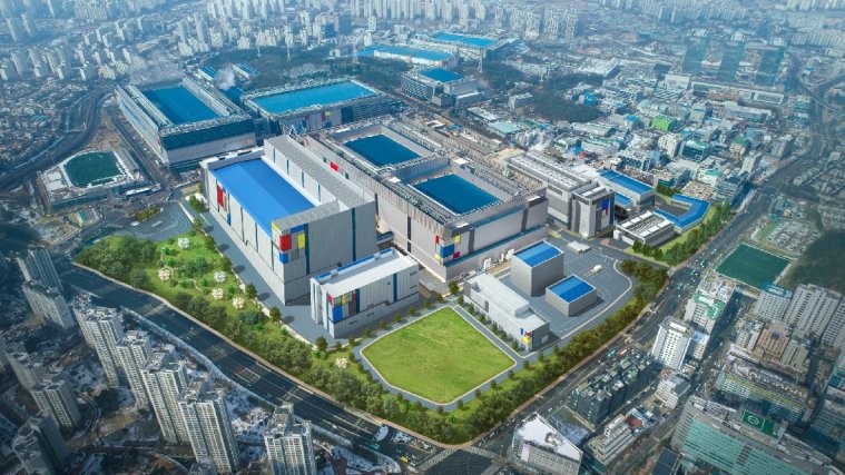
The company also plans to expand its production line to a new EUV line based in Hwaseong, Korea which is expected to be complete by the end of 2019. Currently, their EUV based process technology is manufactured at the S3 line in Hwaseong itself.
According to Charlie Bae, Executive Vice President of Foundry Business at Samsung, “In response to customers’ surging demand for advanced process technologies to differentiate their next-generation products, we continue our commitment to accelerating the volume production of EUV-based technologies.”
Meanwhile, today, Samsung is in the process of launching its Galaxy S10 5G on Verizon, while also solving problems some users are facing on its Galaxy S10 and S10+ handsets. FYI, the S10 5G scored the maximum marks in DxOMark in the camera performance today, which is quite astonishing given how many users actually prefer Pixel over a Samsung nowadays.